Two of the most influential companies in producing the guts of information technology — the chips and gadgets underlying the digital economy and cloud services — are touting advances that are transforming their traditional production processes.
Apple’s specific milestone — its first purchase last week of aluminum produced commercially using carbon-free smelting technology developed by industry giants Alcoa and Rio Tinto — relates to a quest it began almost three years ago to address the carbon footprint of a core component for its enclosures. The joint venture that produced the material is Elysis, a Montreal-based organization backed with more than $144 million, including $10 million from Apple.
Although Apple didn’t disclose how much of the material it purchased, or what it paid, this is more than a test batch — the material was produced in Pittsburgh, but Elysis is ramping up operations in Pennsylvania, Quebec and France. Full-scale commercialization is anticipated around the 2024 timeframe.
“This first sale is tangible evidence of revolutionary work to transform and disrupt the conventional smelting process by making a process that is both more efficient and more sustainable, eliminating all carbon and emitting pure oxygen,” said Ben Kahrs, senior vice president of R&D and manufacturing excellence for Alcoa.
Aluminum is used across the range of Apple products, including its MacBook notebook computers, the Apple Watch and iPhone.
As of 2018, the greenhouse gas emissions associated with manufacturing Apple aluminum represented about 24 percent of its production footprint. According to the company’s 2019 environment report (PDF), it has reduced the impact for some of its MacBook models by more than six times since 2015.
“We’ve done this by sourcing aluminum from hydro-powered smelters, improving the material efficiency of manufacturing processes, and increasing recycled content in our products,” the company wrote. “And by using 100 percent recycled aluminum for the enclosure of the new MacBook Air with Retina display, we cut the product’s carbon footprint in half.”
Intel’s longtime, ongoing quest for circularity
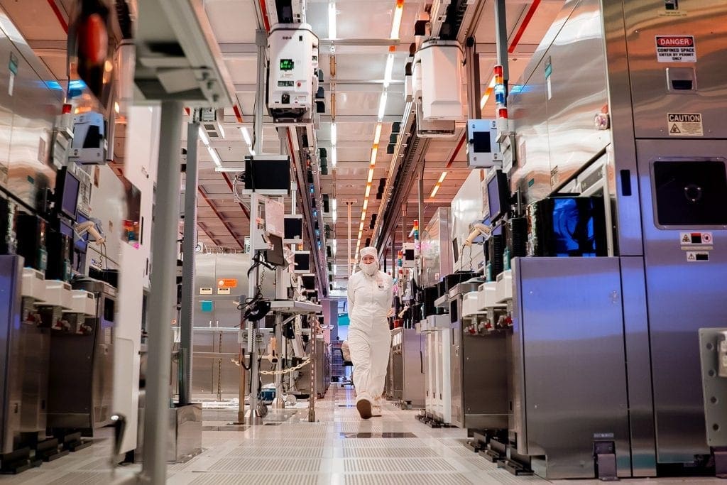
The progress made by Intel relates to its decades of operational focus on reducing waste across its manufacturing operations: since the mid-1990s, it has increased its recycling rate from 25 percent to 90 percent. Since 2015 alone, it has increased the percentage of waste reused and recovered by 275 percent across the company, according to a recently published white paper (PDF) on the topic.
That metric covers all of the waste created within Intel’s operations, such as plastics, food and organics, and what’s generated within its offices in the general course of doing business. But a large majority of the stuff in question are manufacturing waste streams including lithography-related solvents (used to imprint the circuitry onto ships), metal plating waste, specialty base cleaners, spent sulfuric acid, ammonium sulfate and calcium fluoride.
Almost one-fifth of the company’s roughly 110,000 employees are involved in manufacturing. Intel has made “significant” capital investments along the way to accommodate new design and new waste management approaches — think billions of dollars — in its facilities in Arizona, New Mexico, Oregon, Ireland, China and Israel during that multiyear timeframe.
Intel’s vertical integration — it primarily manufactures and designs its products in its own facilities — was key to its ability to rethink its processes, said Kathleen Fiehrer, an Intel materials engineer who has been directly involved in many advances orchestrated over the past seven years.
Some things Intel talks up in its white paper are practices that have become pretty commonplace in the industry. One example: Intel used to send the water (or “bath”) used for creating transistors and interconnects off site to be cleaned up. Now it handles the processes of electroplating more closely, recovering scrap copper that it can resell. This year, the company’s Oregon site is expected to recover more than 600 tons of metal that will be sold on the metals commodity market.
The company chose to invest in handling that process more closely because of the volume of materials involved, as well as the potential value of reselling the materials, Fiehrer said.
Another reuse practice in place for the past six years at its Oregon and Arizona facilities centers on how Intel handles the ammonium wastewater produced when it “washes” the wafers. At those facilities, the company treats the substance to reduce the nitrogen content and then works with an unnamed outside partner to turn it into fertilizer. So far, more than 35,000 tons of ammonium sulfate has been directed into fertilizer. “Keeping that material in the marketplace reduces the amount of energy that would be needed to produce it,” Fiehrer noted.
One of Intel’s latest manufacturing innovations, one that introduces true circularity into the process, centers on how it handles sulfuric acid waste from cleaning. The company began collecting the substance at its Octotillo, Arizona, site in 2017. Last year, it began sending the acid waste to an offsite facility where it is reprocessed to technical grade in quality. Some of that material is then re-sent back to its operations in Arizona and New Mexico, where it can be used in wastewater treatment.
“Our holy grail is to purify a waste stream and take it back on the facilities side or use it on the front end,” Fiehrer said.
Make no mistake: Intel didn’t accomplish these things by itself. It works with thousands of suppliers. While the company doesn’t talk about which partners have helped with which processes, in March, it recognized 35 organizations as key to its continuous process improvement during 2018. “Very few companies get this award,” she noted. One company in particular, Veolia, is cited for “extracting value out of waste resources.” It has received that recognition for the past six years running.
Source: GreenBiz


